Category Archives: applications

First 3D pen

The world’s ‘first 3D pen’ or just a toy?

6 September 2013 Last updated at 15:47 BST,

The creator of 3Doodler claims that the device is the “world’s first 3D drawing pen”.

The pen, according to Mac Bogue, can provide an “introduction” or “companion” to 3D printing.

Mr Bogue demonstrated the pen to Technology correspondent Rory Cellan-Jones at Berlin’s IFA trade show.

[http://www.bbc.co.uk/news/technology-23990597]

As long as the resolution can be increased, should be a fast fabrication tool for making polymer devices.

Atoms star in ‘world’s smallest movie’ – BBC

[http://www.bbc.co.uk/news/science-environment-22358861]

1 May 2013 Last updated at 09:42

A film using single atoms to animate a boy playing with a ball, dancing, and bouncing on a trampoline, has become the world’s smallest stop-motion movie.

The 90-second film, made by IBM, is so small it can only be seen when magnified 100 million times.

The ability to move single atoms is vital for research into data storage at the atomic level – something researchers say could increase the amount of information storable on a device by tens of thousands of times.

Video courtesy of IBM research

http://www.bbc.co.uk/news/science-environment-22358861

http://www.youtube.com/watch?v=CfjWNFwP-HA

Dual suspended core optical fibre for sensing application

Dual suspended core optical fibre

Dual suspended core optical fibre was fabricated and demonstrated by researchers at the Optoelectronics Research Centre in the UK. This fibre has unique function that any other fibres not able to achieve easily, not only transmit light, also the two cores can mechanically move and interact with each other. This MEMS-type of optical fibre was made from lead silicate glass.

The submicron optical fibre is highly sensitive to pressure, vibration etc. and would offer interesting applications in the broad field of sensing.


[http://www.osa.org/about_osa/newsroom/newsreleases/2012/new_dynamic_dual-core_optical_fiber_enhances_data/]

Nanofiber borate bioglass, Cotton candy-like fibers repair wounds

Nanofiber borate bioglass, Cotton candy-like fibers repair wounds

Hard-to-heal open wounds may have met their match in the form of a cottony glass material developed at Missouri University of Science and Technology.

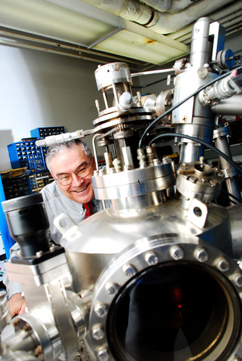
Dr. Delbert Day’s work with glass fibers may lead to a new method to heal open wounds. (Photo by B.A. Rupert/Missouri S&T.)

The glass fiber material could become a source of relief for diabetics fighting infections. It also could be used by battlefield medics or emergency medical technicians to treat wounds in the field.


In a recent clinical trial, the material was found to speed the healing of venous stasis wounds in eight out of the 12 patients enrolled in the trial. Details about the trials and the material were published in the May issue of theAmerican Ceramic Society‘sBulletin magazine.

The material – a nanofiber borate glass – was developed in the laboratories of Missouri S&T’s Graduate Center for Materials Research and the Center for Bone and Tissue Repair and Regeneration, says Dr. Delbert E. Day, Curators’ Professor emeritus of ceramic engineering and a pioneer in the development of bioglass materials. Day and his former student, Dr. Steve Jung, developed the material over the past five years.

Other bioactive glass materials are formed from silica-based glass compositions and have been used primarily for hard-tissue regeneration, such as bone repair. But Day and Jung experimented with borate glass, which early lab studies showed reacted to fluids much faster than silicate glasses.

“The borate glasses react with the body fluids very quickly” when applied to an open wound, says Day. “They begin to dissolve and release elements into the body that stimulate the body to generate new blood vessels. This improves the blood supply to the wound, allowing the body’s normal healing processes to take over.”

Clinical trials at Phelps County Regional Medical Center in Rolla began in the fall of 2010 with 13 subjects. One dropped out early in the process. All suffer from diabetes and had wounds that had been unhealed for more than a year.

Depending on the severity of the wound, Day says the wounds can heal within a few weeks to several months after the material is applied. “Within a few days, most patients see an improvement,” he says.

The material is produced at Mo-Sci Corp., a glass technology company founded by Day. Jung is a glass scientist at the company and holds bachelor’s and master’s degrees in ceramic engineering and a Ph.D. in materials engineering from Missouri S&T.

“Rolla is extremely fortunate to have the three key ingredients needed to take research from the idea stage to the commercial product stage,” says Day, who also invented TheraSphere, a glass product now used to treat patients with liver cancer at more than 100 sites worldwide, including Barnes Jewish Hospital in St. Louis. “We have the university, which provides the research expertise, Phelps County Regional Medical Center for the clinical trials, and Mo-Sci for the manufacturing and commercialization.”

Day foresees expanding the clinical trials to include patients with other types of wounds, such as burn victims.


http://news.mst.edu/2011/05/cotton_candy-like_fibers_repai.html


Glass story—Corning

Watch and share “A Day Made of Glass 2: Unpacked,” to see how Corning’s highly engineered glass, with companion technologies, will help shape our world. Take a journey with our narrator for details on these technologies, answers to your questions, and to learn about what’s possible — and what’s not — in the near future.

Here is the question, how much does Corning contribute to those charming technology? Is that the glass only choice?


Li-Fi, Wi-Fi replacement?

Researchers have used rapid pulses of light to transmit information at speeds of over 500 megabytes per second  at the Heinrich Hertz Institute in Berlin. Dubbed Li-Fi (not to be confused with Light Fidelity) is this a viable competitor to conventional wifi ?

“At the heart of this technology is a new generation of high-brightness light-emitting diodes” says Harold Hass from the University of Edinburgh ”Very simply, if the LED is on, you transmit a digital 1, if it’s off you transmit a 0. They can be switched on and off very quickly, which gives nice opportunities for transmitting data.”

It is possible to encode data in the light by varying the rate at which the LEDs flicker on an off to give different strings of 1s and 0s. The modulation is so fast that the human eye doesn’t notice.

“There are over 14 billion light bulbs world wide, they just need to be replaced with LED ones that transmit data”.

This may solve issues such as the shortage of radio-frequency bandwidth and also allow internet where traditional radio based wireless isn’t allowed such as aircraft or hospitals. One of the shortcomings however is that it only work in direct line of sight.

[http://the-gadgeteer.com/2011/08/29/li-fi-internet-at-the-speed-of-light/]

Will Li-Fi be the new Wi-Fi?

FLICKERING lights are annoying but they may have an upside. Visible light communication (VLC) uses rapid pulses of light to transmit information wirelessly. Now it may be ready to compete with conventional Wi-Fi.

“At the heart of this technology is a new generation of high-brightness light-emitting diodes,” says Harald Haas from the University of Edinburgh, UK. “Very simply, if the LED is on, you transmit a digital 1, if it’s off you transmit a 0,” Haas says. “They can be switched on and off very quickly, which gives nice opportunities for transmitting data.”

It is possible to encode data in the light by varying the rate at which the LEDs flicker on and off to give different strings of 1s and 0s. The LED intensity is modulated so rapidly that human eyes cannot notice, so the output appears constant.

More sophisticated techniques could dramatically increase VLC data rates. Teams at the University of Oxford and the University of Edinburgh are focusing on parallel data transmission using arrays of LEDs, where each LED transmits a different data stream. Other groups are using mixtures of red, green and blue LEDs to alter the light’s frequency, with each frequency encoding a different data channel.

Li-Fi, as it has been dubbed, has already achieved blisteringly high speeds in the lab. Researchers at the Heinrich Hertz Institute in Berlin, Germany, have reached data rates of over 500 megabytes per second using a standard white-light LED. Haas has set up a spin-off firm to sell a consumer VLC transmitter that is due for launch next year. It is capable of transmitting data at 100 MB/s – faster than most UK broadband connections.

Once established, VLC could solve some major communication problems. In 2009, the US Federal Communications Commission warned of a looming spectrum crisis: because our mobile devices are so data-hungry we will soon run out of radio-frequency bandwidth. Li-Fi could free up bandwidth, especially as much of the infrastructure is already in place.

“There are around 14 billion light bulbs worldwide, they just need to be replaced with LED ones that transmit data,” says Haas. “We reckon VLC is a factor of ten cheaper than Wi-Fi.” Because it uses light rather than radio-frequency signals, VLC could be used safely in aircraft, integrated into medical devices and hospitals where Wi-Fi is banned, or even underwater, where Wi-Fi doesn’t work at all.

“The time is right for VLC, I strongly believe that,” says Haas, who presented his work at TED Global in Edinburgh last week.

But some sound a cautious note about VLC’s prospects. It only works in direct line of sight, for example, although this also makes it harder to intercept than Wi-Fi. “There has been a lot of early hype, and there are some very good applications,” says Mark Leeson from the University of Warwick, UK. “But I’m doubtful it’s a panacea. This isn’t technology without a point, but I don’t think it sweeps all before it, either.”


[http://www.newscientist.com/article/mg21128225.400-will-lifi-be-the-new-wifi.html]

Optical Buffer

Today, computer network consist of optical fibre links, interconnected by electrical nodes. The data transport in the backbone is done in the form of light (Laser etc.) Dense wavelength division multiplexing (DWDM) technologies enable bitrate well beyond 1 Tbit/s. however, at the nodes; this light has to be converted to the electronic domain, in order to switch all data to their separate destinations. Due to rapidly increasing channel capacities, the switching capacity is becoming bottleneck of the system. Currently, research activities focus on optical switching technologies that involve fewer or no conversions from the optical to the electronic domain. An important problem is the buffering.

An optical buffer is a device that is capable to temporarily store light; it serves to store data that was transmitted optically without converting into electronic domain.

[wikipedia: Optical buffer. http://en.wikipedia.org/wiki/Optical_buffer%5D

E-book display business [Nature Photonics]

E Ink Holdings (Hsinchu, Taiwan, world’s largest supplier of displays to the e-book market), whose power-efficient display technology is used in the Amazon Kindle as well as a range of other electronic book (e-book) readers, says sales of its products nearly doubled in the last quarter of 2010. [Nature Photonics, 2011, Business News]

Chalcogenide glass, tellurite glass, bismuth glass, lead-silicate glass (schott), ZBLAN, silica, anything else?

Chalcogenide glass, tellurite glass, bismuth glass, lead-silicate glass (schott), ZBLAN, silica, anything else?

well, quite a long name. the title lists the recent popular glasses that used in fibre optics application.

Bragg layer, 1D optical crystal fibre

Historically the 1D photonic crystal has been known as the Bragg reflector or mirror, a periodic structure composed of two alternating layers of thickness t=\lambda/4n, where n is the refractive index of the layer and lambda is the free space wavelength for which optimal reflection has been designed.[Y. Yi, http://photonics.mit.edu/Photonic_Crystals.html%5D

A popular example of a photonic crystal device is the photonic crystal fiber, successfully demonstrated by Fink, Joannopoulos et al. at MIT. The ‘Omni guide’ fibre were fabricated using a bilayer (polymer and AsSe glass).[Nature 420, 650-653 (12 December 2002)]

The first demonstration of a photonic crystal waveguide, a planar-processed version of this device, developed by the EMAT group (see in figure). Comprised of a conformal cladded 1D Si/Si3N4photonic crystal; the waveguide core is a defect layer of SiO2.[Y.Yi]

Also, other groups (http://www.4spepro.org/view.php?article=002597-2010-02-05) demonstrated the fabrication of Bragg layer waveguide in polymer.

The future challenge will be demonstration of Bragg-layer fibres in all-glasses.